LANCOM NWAPP
aka. L-320agn Wireless, L-321agn Wireless, L-322agn dual Wireless_
This is the original design; for the redesigned version see NWAPP2.
Pictures

LANCOM NWAPP.E0, top side
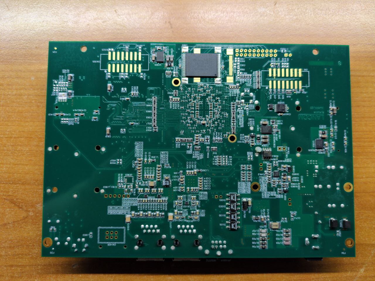
LANCOM NWAPP.E0, bottom side
- LANCOM console port (RS-232 over mini-DIN 8-pin)
- 10/100/1000 Mbit/s Ethernet port
- 10/100 Mbit/s Ethernet port
- 12 V DC
- 2 mPCIe slots for WLAN
Top side:
- U1: Freescale MPC8314E SoC - powerpc 32-bit, PowerQUICC II, e300 core
- U800, U801: Nanya NT5DS16M16DS-ST: 256Mb DDR SDRAM (64 MiB in total)
- U1001: Marvell 88E1116-NNC1: Gigabit Ethernet PHY
- U1101: Marvell 88E3018-NNC1: "Fast" Ethernet PHY (100 Mbit/s)
- U401: TI SN74LVCH16373A: 16-Bit Transparent D-Type Latch With 3-State Outputs
- U1500, U1501: TI CDx4HC164: High-Speed CMOS Logic 8-Bit Serial-In, Parallel-Out Shift Register
Bottom side:
- U900: Intel StrataFlash JS28F128: 256 Mbit CFI NOR flash
- JP1500 (
D) is the debug jumper. Setting it causes the bootloader to skip the memory test and start the main menu instead of any installed firmware. - CN1500 is for flash access
- CN1501 ?
- CN1 is for JTAG, it follows the JTAG/COP pinout:

V<adr>/I/R/G/B/S/U/D/e/f/t/H/?>
Flashlayout:16MB_Strataflash
 FE000000      32KiB Loader1
 FE008000       8KiB Romdscr1
 FE00A000      24KiB Unused
 FE010000       8KiB Romdscr2
 FE012000      24KiB Unused
 FE018000     160KiB Loader2
 FE040000     512KiB LCFS
 FE0C0000     512KiB Config
 FE140000     512KiB Accounting
 FE1C0000   14592KiB Firmware
V<adr>/I/R/G/B/S/U/D/e/f/t/H/?>

Monitor help page
-----------------
 V<adr>  : Dump memory addresses <adr>
 G       : Start active firmware
 I       : Version Info
 U0,U1   : Upload file to Flash-ROM by XMODEM-/CRC
 D0,D1   : Download file by XMODEM-128/1K
 R       : Reboot (Warmstart)

 Bx      : Modify outband bitrate

 E ...*  : Erase menu       * = action required
 F ...   : Firmware menu
 T ...   : Test menu
Memory (both RAM and flash) can be dumping with two simple scripts:
decode.py
#!/usr/bin/python3
import re, argparse

LINE = re.compile("(........):  (.. .. .. .. .. .. .. ..  .. .. .. .. .. .. .. ..) | ................")
MiB = 1024 ** 2

def main(i, o):
    buf = bytearray()
    start = None
    for line in i:
        if 'L2Ldr: exception #' in line: break
        if m := LINE.match(line):
            addr = int(m.group(1), 16)
            if not start:
                start = addr
                print(f"Start: {start:#x}")
            offset = addr - start
            data = bytes.fromhex(m.group(2))
            if len(buf) < offset:
                buf += b'\0' * (offset - len(buf))
            if len(buf) != offset:
                print("vorwärts immer, rückwärts nimmer!")
                break
            buf += data
    l = len(buf)
    print(f"Got {l} ({l:#x}) bytes, {l / MiB:.4} MiB")
    o.write(buf)


if __name__ == '__main__':
    parser = argparse.ArgumentParser(description="decode LANCOM bootloader output")
    parser.add_argument('log', help='log file to read')
    parser.add_argument('bin', help='binary file to write')
    args = parser.parse_args()
    i = open(args.log, 'r')
    o = open(args.bin, 'wb')
    main(i, o)
trigger.sh
#!/bin/sh
printf "V$1\r"
while sleep 0.1; do printf '\r'; done
which are then invoked like this:
./trigger.sh 0 | microcom -s 115200 /dev/ttyUSB0 | tee ram.log
./trigger.sh FE000000 | microcom -s 115200 /dev/ttyUSB0 | tee flash.log
./decode.py ram.log ram.bin
./decode.py flash.log flash.binThe test menu can be entered by pressing t in the main menu.
It offers a shell-like interface, rather than the single-letter commands in the
main menu.
V<adr>/I/R/G/B/S/U/D/e/f/t/H/?>

If you can read this, you have voided your warranty.
Mon>help
help>
unknown command! type ? for help

Mon>?
?>
fs_list                                           list filesystem contents
fs_del       <id>                                 delete file <id>
list_flash                                        detect/list flash roms
q                                                 Quit
;                                                 queue commands
run          <num>                                start firmware #num (0 or 1)
dbg          <dbg_lvl>                            Set debug level 0..n (default==1)
rep          <val>; cmd <args> [;cmd <args>] ...  repeat commands n-times
cb           <addr32>, <data8>                    read and compare byte value from address
cw           <addr32>, <data16>                   read and compare word value from address
cl           <addr32>, <data32>                   read and compare long value from address
rb           <addr32>                             read byte value from address
rw           <addr32>                             read word value from address
rl           <addr32>                             read long value from address
wb           <addr32>,<data8> [,count]            write byte value to address
ww           <addr32>,<data16> [,count]           write word value to address
wl           <addr32>,<data32> [,count]           write long value to address
test_timers                                       test timer system
test_wdog                                         test watchdog
v24_status                                        show V24 status lines
v24_dcd      1|0                                  set V24 DCD signal
v24_dsr      1|0                                  set V24 DSR signal
upload                                            upload UPX-File to flash(X-Modem)
download     start,end                            X-Modem download
led          num,val                              test LED
?                                                 Help
coldboot                                          cold-boot system (if implemented)
d            [base[,len]]                         dump memory block
mmu                                               print mmu regs
clocks                                            print clocks
map                                               print mappings
cr           hostbrg,bus,dev,fct,reg [,data32]    read and optionally compare PCI config reg
cw           hostbrg,bus,dev,fct,reg,val          write PCI config reg
lspci                                             list PCI devices

Mon>
The file system uses numerical tags instead of names:
Mon>fs_list
fs_list>
FE040004: ID 5, len 00000039
FE040040: ID 4, len 00000072
FE0400B5: ID 1, len 0000E29F
FE04E357: ID 12, len 0000068B
FE04E9E5: ID 41, len 0000068B
FE04F073: ID 43, len 0000029C
FE04F312: ID 47, len 000000F1
FE04F406: ID 3, len 00000074
FE04F47D: ID A9, len 00001216
FE050696: ID D, len 00000004
FE068FEE: ID 6, len 0000B850
FE07595B: ID C7, len 000007A9
FE076107: <END>
GPIODAT = 0xe0000c08
| number | mask | device | description |
|---|---|---|---|
| 2 | 0x2000_0000 |
bitbanged latch | |
| 5 | 0x0400_0000 |
bitbanged clock | |
| 16 | 0x0000_8000 |
JP1500 | debug status (active low) |
| 17 | 0x0000_4000 |
SW1500 | reset button (active low) |
| 18 | 0x0000_2000 |
something related to SPI | |
| 20 | 0x0000_0800 |
bitbanged data | |
| 21 | 0x0000_0400 |
RS-232 DCD active | |
| 22 | 0x0000_0200 |
RS-232 DSR active |
The MPC8314E has 32 GPIOs. Their usage on the NWAPP2 board is as follows, (#) indicates active low signals:
An 8-bit shift register is bitbanged through GPIO 2/5/20. Bits are transmitted MSB-first, in the following steps:
- clock, latch, data = 0
- for every bit:
- data = bit
- clock = 1
- clock = 0
- latch = 1
- latch = 0
| number | mask | default | description |
|---|---|---|---|
| 0 | 0x01 |
1 | |
| 1 | 0x02 |
1 | |
| 2 | 0x04 |
0 | |
| 3 | 0x08 |
1 | |
| 4 | 0x10 |
1 | |
| 5 | 0x20 |
0 | |
| 6 | 0x40 |
0 | board reset |
| 7 | 0x80 |
0 |
The LEDs are connected to the shift registers U1500/U1501, which are driven
through the SoC's SPI controller. LANCOM's bootloader configures the SPI
controller to use 16-bit words, so that a single word-write to the SPI transmit
register at 0xe0007030 sets the LED pattern. The shift registers do not have
a latch pin, so any changes come into effect immediately.